Product Brands
Automatic Optical Inspection (AOI)
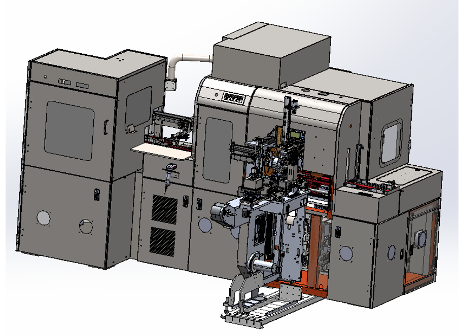
Precision Machining in Semiconductor Advanced Packaging
Leader in Thermal and UV Light Process Equipment since 1966
High Resolution 3D Surface Non-Contact Measurement Systems
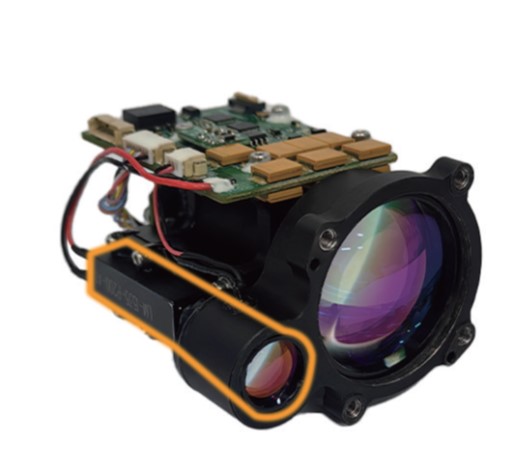
Laser Range Finder
Auto and Accurate Bond Tester
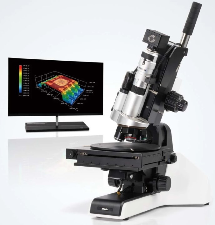
Microscopy Solution - More than Microscopy
High End 3D CT X-Ray
Wafer Inspection Systems
Reflow Simulator for Observation and Measurement
Scanning Acoustic Microscopy Analytical Systems
Nikon XTV160 Xray
Reliable High Speed Test Handlers since 2011
Microwave Plasma Decapsulation System
eviXscan 3D is a brand of high quality scanners based on structured light technology
Electron Microscope Supplies
Full solution of Metallography, Metallurgical Testing, Microstructural Analysis
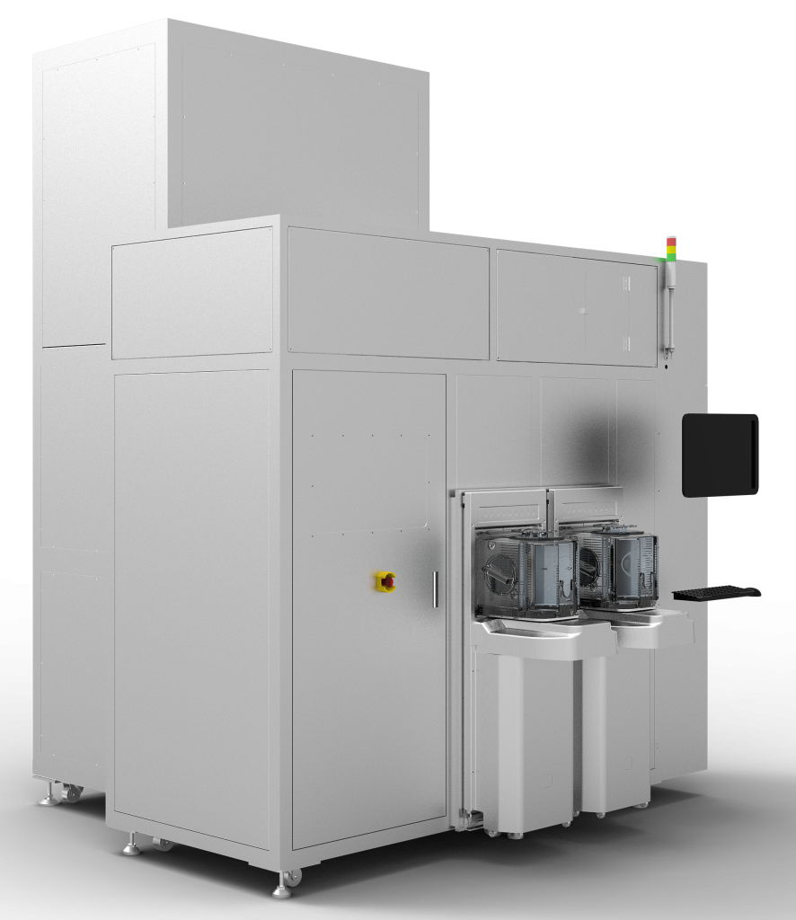
Leader in Wafer AOI and Precision Grinding in Semiconductor Advanced Packaging
- Brand
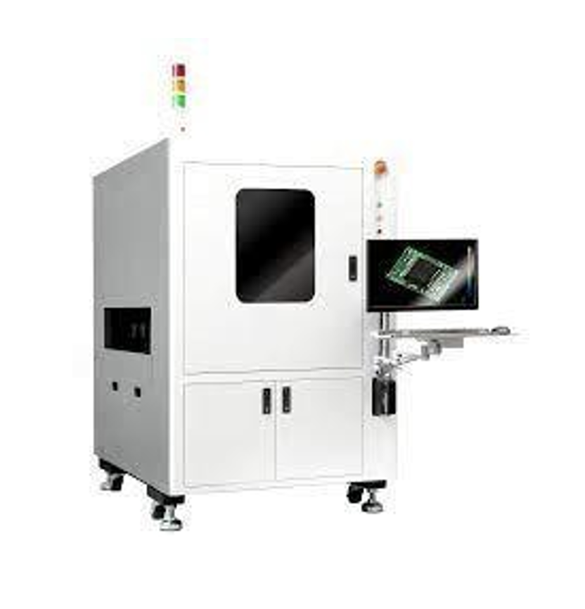
- Symphony AOI
HW 5010TR and HW 5010TT
Applied after final test, it can detect appearance defects in encapsulated devices by patented 2D/3D vision inspection system.


- Brand
- UHS 3D CT Xray
XVA 160RZ
High resolution 3D X-ray CT system Versatile MicroFocus model, perfect for inspection & analysis of SMT boards or other items.

- Brand
- UHS 3D CT Xray
XVA 160 Alpha II Z
3D X-ray CT system High-end Nano-focus model, ideal for inspection & analysis of semiconductors & electronic components.

- Brand
- Muegge
STP 2005
Plasma Decapsulation Tool Microwave Plasma System with integrated Remote Plasma Source

- Brand
- Motic
Easy Zoom Digital Microscope
A flexible, high performance digital microscope that is well suited for material inspection. The microscope offers 50x to 5800x magnification in a single zoom body, providing extreme versatility and making it a great fit for any application.
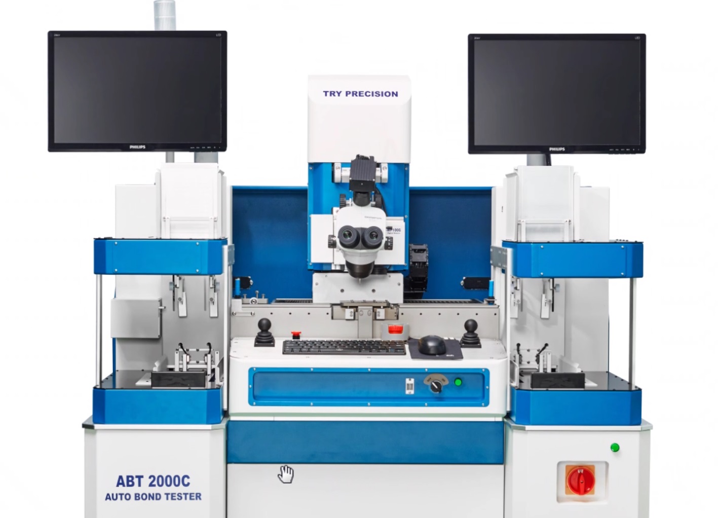
- Brand
- TRY Precision
ABT2000C
Fully Automatic Bond Tester for Wire Pull, Ball Shear , Die Shear with Automatic Leadframe/Substrate Loader

- Brand
- PVA TePla SAM
SAM 302 TWIN
SAM system that utilizes arrays of two transducers to acquire simultaneous acoustic images

- Brand
- PVA TePla SAM
SAM 301 HD2
Most popular customer choice for high performance failure analysis in both production and R&D environments
- Brand
- Symphony AOI
HW Wafer AOI 5510
Applied to shipment after wafer cutting/post-seal cutting, it detects um-level defects on 6-12 inch wafers, provides yield feedback and outputs map to optimize efficiency