Applications
Wafer Fabrication to Backend Packaging
Interfacial characterization of Ultra-Thin Films, Transparent FIlms and Thick Fim
Metals, Ceramics, Polymers and Composites
Structural & Cell Biology , Pharmaceuticals, Medical Implants & Devices, Biomimetics, and Pathology
Various General Industry Application
Sample Preparation for SEM

- Applications
- Semiconductor & Electronics
Mostrak 2 for Back End Testing
Back end Testing for Packaged Devices

- Applications
- Semiconductor & Electronics
3D XRay CT on Semiconductor TSV and Wire Bond
5um TSV , Solder Bump Crack and Wire Bonding

- Applications
- Semiconductor & Electronics
cyberTECH for Wafer Laser Groove Depth and Width Auto Measurement
Laser Dicing Depth and Width Auto Measurement

- Applications
- Semiconductor & Electronics
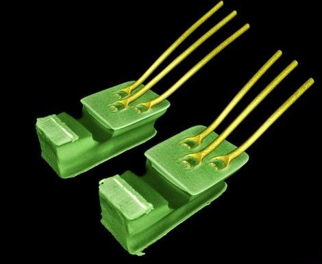
Phenom XL for Wire Bond and Whisker Inspection
Phenom XL provides 100 x 100mm stage with flexibility to inspect wire bond with EDS in either QC, R&D , Production or Failure Analysis

- Applications
- Semiconductor & Electronics
cyberTECHNOLOGIES for Semiconductor Application
High-resolution, non-contact 3D measurement system options to the microelectronics

- Applications
- Semiconductor & Electronics
PVA TEPLA SAM for Semiconductor Application
Non destructive inspection of delamination or void

- Applications
- Semiconductor & Electronics
DITECT for Semiconductor Application
High Speed Imaging of Wire Bond Process
